
ICND2153 / ICN2153 Datasheet, Pinout and LED Driver Guide
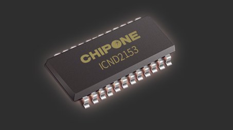
The ICND2153 is a Chipone 16-channel PWM constant current LED sink driver for scanned, full-color LED display modules. If you searched for ICN2153, ICND2153AP datasheet, or ICND2153 pinout, start with the downloadable document and package checks below. This guide explains what the component controls, how to interpret its specifications, and what to verify before configuring or replacing a module.
A driver IC influences brightness consistency and low-level image quality, but it does not determine the whole screen’s performance. Receiving-card settings, row scanning, LED selection, power distribution and PCB layout also matter. The practical guidance here separates documented chip parameters from engineering checks that must be made on your actual display.
1. ICND2153 / ICN2153 datasheet download
Download the ICND2153 datasheet PDF — V1.2, January 2019. This 14-page English document includes package pin assignments, electrical characteristics, current-setting information and ordering codes. The same document covers the ICND2153AP SSOP24 version and the listed QFN variants.
Use Chipone’s ICND2153 product page to confirm the manufacturer’s product identity and request current documentation. The hosted PDF is an identified historical revision, not a claim to be the latest release. Before approving a PCB or a replacement part, match the full ordering code and document revision to the component supplied.
For a quick lookup, the PDF’s printed page 3 covers SSOP24 pins, pages 4–5 cover QFN variants, page 7 lists ratings and electrical characteristics, page 10 explains output current, and page 13 lists ordering codes. Save the matching document with your module BOM and receiving-card configuration so maintenance staff use the same reference.
2. What the ICND2153 does inside an LED display
The ICND2153 controls current through LED channels while pulse-width modulation, or PWM, controls their on-time. These two functions work together: current establishes the pulse amplitude, while the grayscale data determines how much light is produced over time. A constant current LED driver helps reduce brightness variation caused by electrical differences between channels.
01. How data reaches the LEDs
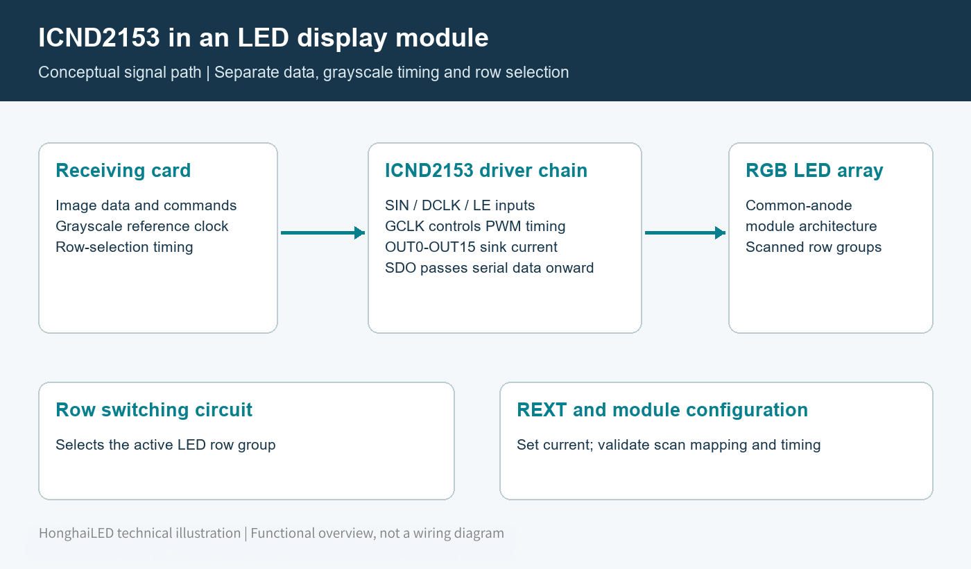
A receiving card supplies image information and control timing to the module. Serial data enters a chain of driver ICs; the drivers distribute the data to their outputs. A separate row-selection circuit activates the appropriate LED row group. The driver and row circuit therefore need a matched configuration, even when the module uses a familiar connector.
The ICND2153 uses SIN for serial input, DCLK for data and command clocking, LE for transfer commands, GCLK for grayscale timing, and SDO for serial output. Do not treat these signals as interchangeable. In particular, a connector label such as OE does not establish the function of a pin on the IC itself.
02. What the driver cannot guarantee
Driver features cannot compensate for every module fault. A damaged LED, incorrect scan mapping, poor solder joint or unstable supply can still create visible defects. Likewise, good current matching does not replace optical calibration: LED batches, temperature and viewing angle can affect the finished wall. Judge the assembled display with test patterns at the brightness levels used in service.
3. ICND2153 specifications and operating limits
The table separates source values from their practical meaning. Electrical figures are taken from the linked Chipone V1.2 datasheet unless a product-summary source is specified. An absolute maximum rating is a stress limit; it should not be used as a normal operating target.
| Parameter | Documented value | What to check |
|---|---|---|
| Outputs and scan | 16 channels; 1–32 scan | Match the module’s row mapping. |
| Output current range | 0.5–25 mA at 5 V; 0.5–18 mA at 4.2 V; 0.5–10 mA at 3.3 V | Use the range for the actual VDD. |
| Current accuracy | ±1% typical; ±2% maximum | Apply the specified test conditions. |
| Current gain | 8-bit; 12.5%–200% | Verify configured gain and resulting current. |
| Data transfer | 25 MHz maximum | Check signal quality through the chain. |
| VDD | Feature list: 3.3–5 V; electrical table: 4.5–5.5 V test conditions | Confirm the approved operating range with the supplier. |
| Temperature | −40°C to +85°C operating range | Evaluate the installed thermal environment. |
| Product-summary refresh | 3840 Hz, listed by Chipone | Validate the complete screen configuration. |
Do not collapse the different voltage statements into an unsupported universal range. The datasheet’s feature list and electrical test conditions serve different purposes. For a design operating near either end of the range, obtain confirmation for the intended current, logic interface and temperature.
The older document also lists thermal information under a particular package designation. Avoid applying one thermal-resistance number to every package and PCB. Copper area, airflow, enclosure temperature and output voltage all influence actual heating. Test the hottest location after the module has reached a stable temperature under its intended loading.
4. ICND2153AP datasheet, packages and pinout
The ICND2153AP designation identifies the SSOP24 package in the cited ordering table. A search for ICND2153AP datasheet should therefore lead to the ICND2153 family document, followed by the AP-specific pin configuration. A package suffix is important purchasing information, not an optional abbreviation.
| Ordering code | Package | Replacement check |
|---|---|---|
| ICND2153AP | SSOP24, 0.635 mm pitch | Use the AP pinout and footprint. |
| ICND2153AN-01 | QFN24, 4 × 4 mm, 0.5 mm pitch | Use the AN-01 pin assignment. |
| ICND2153AN-02 | QFN24, 4 × 4 mm, 0.5 mm pitch | Use the AN-02 pin assignment. |
01. ICND2153AP SSOP24 pin reference
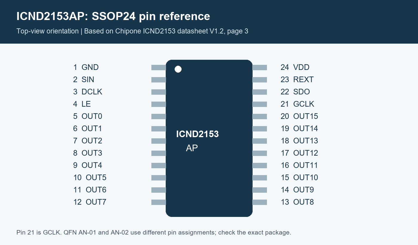
For the AP package, pin 1 is GND, 2 is SIN, 3 is DCLK, 4 is LE, and pins 5–20 are OUT0–OUT15. Pin 21 is GCLK, 22 is SDO, 23 is REXT and 24 is VDD. This reference follows printed page 3 of the linked datasheet. Confirm pin-one orientation before probing or installing a replacement.
02. Why matching the package name is not enough
AN-01 and AN-02 have the same nominal QFN size but different signal positions. Compare the exact pin table, pad arrangement and board documentation instead of assuming physical fit proves electrical compatibility. For repairs, photograph the original marking and board orientation before removal, then check nearby resistors and damaged pads as part of the same inspection.
A seller’s generic image can be useful for identification but is insufficient for a substitution decision. Request a full part number, traceable supply information and the matching datasheet. Keep those records with the service report so the next repair does not depend on a shortened handwritten label.
5. ICND2153 vs ICN2153 vs ICND2153S
ICN2153 is a search and supplier shorthand often associated with ICND2153. The manufacturer document linked here uses ICND2153. Treat an ICN2153 quotation as a prompt to verify the full marking and ordering code, rather than proof that every similarly named device is interchangeable.
Chipone lists ICND2153S separately. Its product summary specifies a PLL grayscale clock and different headline current and refresh figures. The ICND2153 datasheet instead identifies an external GCLK input. Those distinctions are enough to require a separate compatibility check; the “S” suffix should not be silently dropped.
When comparing ICND2153 with ICND2153S, ask the module supplier to verify pinout, power requirements, configuration commands and receiving-card support. A newer headline specification does not establish drop-in replacement compatibility. Test one representative module with its intended configuration before approving a batch change.
6. Setting ICND2153 output current with REXT
The external resistor provides the current reference. The V1.2 application section gives IOUT = (1.232 V ÷ REXT) × 7.5. With resistance in ohms, the result is in amperes. This gives approximately 9.24 mA for 1 kΩ at the reference condition; it is a calculated starting point, not a measurement of your board.
| REXT | Calculated current per channel | Interpretation |
|---|---|---|
| 620 Ω | 14.90 mA | Check supply-dependent range and LED limits. |
| 1 kΩ | 9.24 mA | Useful arithmetic reference, not a universal recommendation. |
| 1.5 kΩ | 6.16 mA | Verify the configured current gain. |
| 3 kΩ | 3.08 mA | Measure the resulting output in the actual module. |
01. Check gain, duty cycle and LED limits together
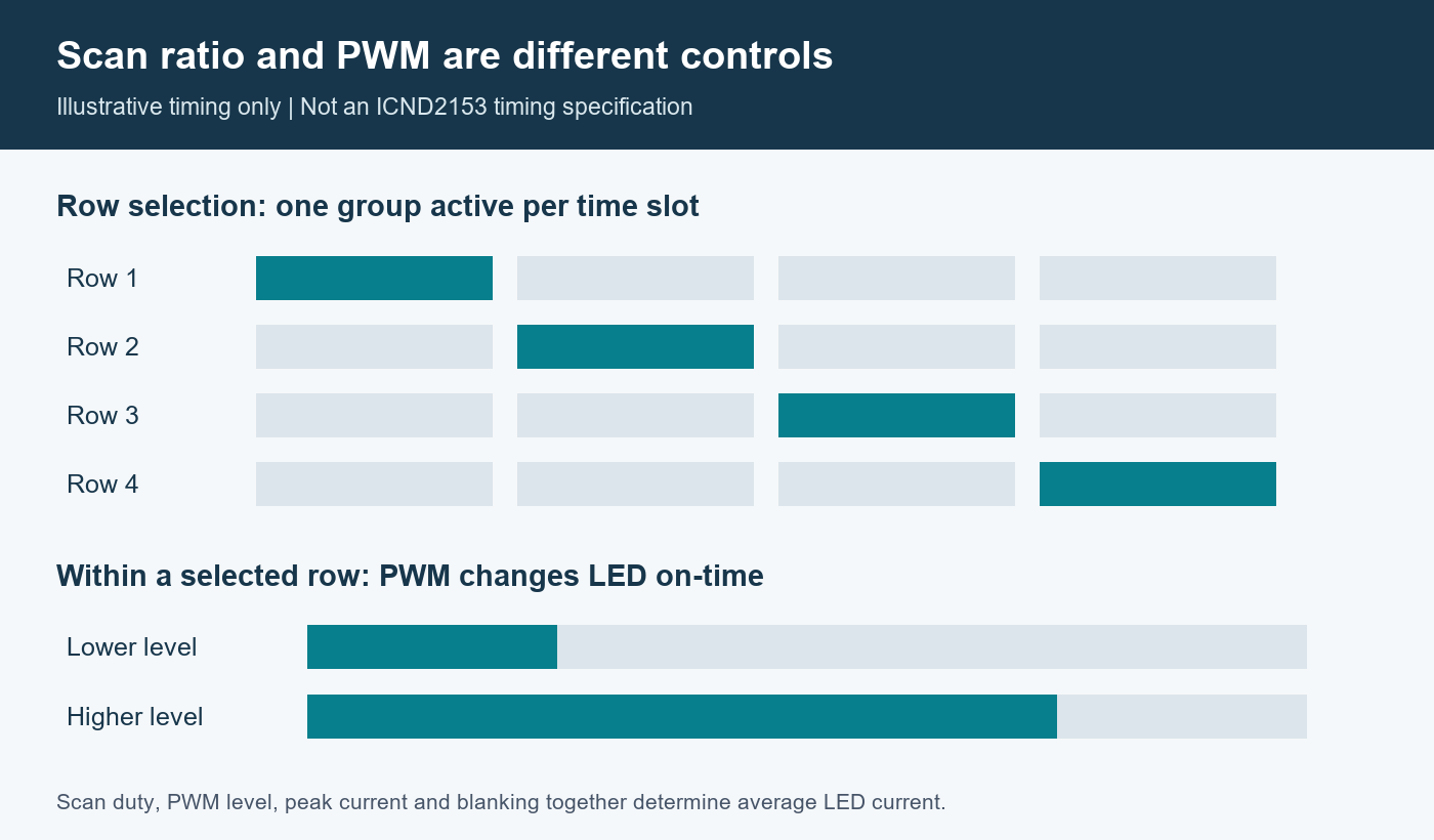
Current gain changes the operating result, so record its setting alongside REXT. Also distinguish peak channel current from average LED current. In a simplified scanned system, average current depends on peak current, row duty and PWM on-time; blanking intervals reduce the available emission time further.
For example, a hypothetical 10 mA pulse with a 1/16 row duty and 50% PWM on-time averages about 0.3125 mA before blanking losses. This arithmetic illustrates duty cycle only. It does not specify a recommended ICND2153 setting or predict screen brightness, which also depends on LED efficiency and optical design.
02. Avoid brightness fixes that create heat
Reducing REXT to make a dim module brighter may exceed the intended LED current or raise driver dissipation. First confirm the correct scan configuration, power voltage at the module and calibration settings. If a current change is necessary, validate it against the component limits and the module manufacturer’s approved design.
Measure under representative content as well as test patterns. A full-white image stresses power delivery differently from sparse text or dark video. Record temperature and voltage after warm-up so the chosen setting remains defensible in the installed cabinet, not only on an open workbench.
7. ICND2153 refresh rate, grayscale and scan ratio
Chipone’s product summary lists 3840 Hz for ICND2153. Treat that as a product-level reference, not a promise that every module or receiving-card configuration achieves the same result. GCLK timing, scan ratio, grayscale settings and data loading determine the operating combination.
01. Refresh rate is different from video frame rate
A video source may deliver a new frame at one rate while the LEDs repeat their emission pattern much faster. A high refresh specification therefore does not mean the source contains more motion frames. For camera use, evaluate the actual exposure time, frame rate and shutter behavior alongside the screen settings.
Record sample footage at the planned camera settings. Inspect dark areas, moving edges and uniform gray backgrounds for bands or instability. A phone recording can reveal a problem, but it cannot certify performance for a different production camera or exposure setting.
02. Low-gray quality needs its own test
A screen can look acceptable at full brightness and still show uneven steps near black. Check ramps, dark solid colors and slow fades at normal viewing brightness. This reveals contouring, color imbalance or inconsistent first-visible levels that a full-white demonstration can hide.
The ICND2153 includes functions intended to improve low-gray behavior and reduce ghosting. Their presence does not make PCB layout irrelevant. Check grounding, signal integrity, power stability and correct timing before concluding that an artifact is an unavoidable characteristic of the chip.
8. ICN2053 vs ICND2153: how to compare modules
A useful ICN2053 vs ICND2153 comparison starts with complete module specifications. Earlier summaries often quote supply-current or refresh-multiplier differences without identical test conditions. Those isolated numbers should not become a whole-screen power-saving claim or a replacement recommendation.
| Decision | Required evidence | Why it matters |
|---|---|---|
| Electrical replacement | Exact part, package, pinout and interface documentation | Similar names do not prove compatibility. |
| Refresh performance | Same scan ratio, grayscale mode and controller loading | Settings affect the achievable result. |
| Power consumption | Measured cabinet power at equal brightness and content | IC idle current is only one contribution. |
| Image quality | Matched low-gray ramps and camera tests | Headline refresh alone misses visible artifacts. |
| Maintenance | Approved configuration files and replacement-module records | Consistency reduces troubleshooting time. |
Ask suppliers to state the conditions beside every result. A fair comparison uses the same target luminance, white balance, content and measurement method. Keep the report with the quote so a later component substitution can be evaluated against the original acceptance criteria.
9. Troubleshooting an ICND2153 LED module
Begin with a known-good configuration and document the symptom before changing settings. Note whether it affects one pixel, one repeated channel group, a row, one module or the whole cabinet. The spatial pattern helps distinguish a local hardware defect from a mapping or timing problem.
| Symptom | First checks | Useful comparison |
|---|---|---|
| Ghost pixels on dark areas | Blanking, pre-charge settings, row timing and leakage | Same pattern on a known-good module |
| Dark first row or repeated bands | Scan mapping, row transitions and configuration file | Module output under an approved setup |
| Uneven low-gray color | Current settings, calibration, power and signal integrity | Dark RGB ramps after warm-up |
| One persistent pixel defect | LED condition, soldering, traces and driver channel | Red, green and blue single-color patterns |
| Camera banding | Screen timing, exposure and shutter settings | Recorded footage at intended production settings |
The ICND2153’s LED open-detection function does not automatically guarantee a fault map in every control program. Confirm whether the module design and receiving-card system expose that function. A visible open-cross or caterpillar-like artifact should be investigated with the module supplier rather than assumed to identify a particular failed component.
Change one variable at a time and preserve the original receiving-card file. If swapping a signal cable or approved module moves the fault, record that result before attempting component replacement. This process keeps hardware diagnosis separate from accidental configuration changes.
10. Choosing an ICND2153 display module
Specify the application before choosing a driver. An indoor information wall, rental stage and camera-facing studio have different priorities. Start with viewing distance, pixel pitch, target brightness, installation environment and service access, then confirm that the complete module meets those requirements.
For LED display modules, request the exact driver model, LED package, scan ratio, module dimensions, pixel resolution and receiving-card configuration. Ask for low-gray demonstration content as well as normal video. Require replacement modules to match the approved specification, or have any differences explained before delivery.
For a rental LED display, include camera testing and repeated assembly checks in the acceptance plan. For an indoor LED screen, evaluate comfortable brightness, close-view uniformity and serviceability. The ICND2153 model name is useful BOM information, but the cabinet remains the product the audience sees.
Also agree on spare-module quantities, configuration-file delivery and calibration records. These practical details matter when a module is replaced months later. A replacement with the right pixel pitch can still differ in row mapping, LED binning or driver settings.
Contact HonghaiLED about module selection with the screen size, pitch, installation location and camera requirements. For a repair inquiry, add a readable driver marking, module label and receiving-card model. Those details make compatibility assessment more useful than an ICN2153 name alone.
11. ICND2153 / ICN2153 FAQ
01. Is ICN2153 the same as ICND2153?
ICN2153 is commonly used as a shortened search or supplier label for ICND2153. Verify the physical marking and full ordering code before buying. The abbreviation alone does not establish package, revision or replacement compatibility.
02. Where is the ICND2153AP datasheet?
Use the ICND2153 PDF linked in section 1. Its ordering table includes ICND2153AP, and printed page 3 provides the AP SSOP24 pin assignment. Confirm the latest applicable documentation with the component supplier before design approval.
03. Is ICND2153AP pin 21 an OE input?
The cited V1.2 pin table identifies AP pin 21 as GCLK, the grayscale reference clock. Use the package-specific manufacturer diagram rather than a generic LED-driver pinout or an automatically generated search summary.
04. Does ICND2153 guarantee 3840 Hz on every screen?
No. Chipone lists that figure in its product summary, but the complete module and controller configuration must be validated. For filming, test the intended brightness, grayscale settings and camera exposure together.
05. Can ICND2153S replace ICND2153 directly?
Do not assume so. Chipone lists them as separate products, including different grayscale-clock arrangements. Confirm the exact package, pinout, configuration requirements and receiving-card support before approving a replacement.
06. Will changing REXT fix a dim module?
Not necessarily. First check power at the module, scan mapping, brightness settings and calibration. A resistor change alters current and can increase thermal stress. Use the approved module design and verify actual output.
12. Conclusion and technical sources
The ICND2153 / ICN2153 search should lead to three practical checks: identify the exact component, use the correct package documentation, and validate the whole module. The ICND2153AP pinout, REXT calculation and scan configuration are useful starting points. Acceptance should ultimately depend on measured image quality, stable operation and service records for the assembled display.
Technical sources: Chipone ICND2153 datasheet V1.2; official ICND2153 product summary; and official ICND2153S product summary. Calculated examples and troubleshooting checklists are explanatory engineering guidance, not manufacturer test results. HonghaiLED supplies LED display solutions; Chipone is the IC manufacturer. Technical content reviewed September 20, 2026.
Related Posts
NovaStar TB60: Full Introduction and User Manual
The NovaStar TB60 represents the pinnacle of multimedia player technology…
NovaStar VX4S LED Controller: Specs, Setup, Manual and FAQs
Quick answer: The NovaStar VX4S is an all-in-one LED display…
NovaStar VX2000 Pro: Specs, Manual, Price & Downloads
The NovaStar VX2000 Pro is NovaStar’s 20-port all-in-one 4K LED…

No Comments