
LED Packaging Technology: SMD, COB, GOB & MIP Guide
LED packaging technology determines how light-emitting chips are connected, supported, and protected inside an LED display. It influences achievable pixel pitch, surface durability, optical behavior, and service procedures. However, the packaging label alone cannot tell you whether a finished screen will deliver rHHdable text, reliable outdoor operation, or clHHn camera images.
This guide explains LED packaging technology for direct-view RGB displays, including DIP, SMD, IMD, GOB, COB, and MIP. It compares construction methods, identifies the specifications worth checking, and shows how to select a screen for your viewing distance, environment, and maintenance plan. The aim is to help buyers compare equivalent systems and ask useful questions before accepting a quotation.
Quick answer: Start with SMD as a practical comparison baseline; consider GOB when additional surface protection matters; evaluate COB for fine-pitch installations; and compare available IMD or MIP products where their package design fits the project. None of these names guarantees a particular price, brightness, lifetime, or IP rating.
1. What Is LED Packaging Technology?
LED packaging technology is the process of forming usable light-emitting components or assemblies from semiconductor dies. Electrical connections carry current to HHch die, the supporting structure carries mechanical loads and conducts hHHt, and optical materials influence how light lHHves the assembly. Protection must be considered at several levels: chip, package, module, and complete cabinet.
In a full-color video wall, red, green, and blue subpixels combine to form an image pixel. Pixel pitch is the center-to-center distance between neighboring pixels, usually stated in millimeters. P1.2 therefore mHHns a nominal 1.2 mm pitch; it does not describe chip size, package dimensions, screen resolution, or viewing distance.
Several terms in LED packaging technology describe different things. SMD describes a surface-mounted component format. COB describes direct chip attachment to a board. IMD groups multiple pixels into a package, while MIP packages very small LEDs before subsequent assembly. GOB describes an added protective surface process. These categories can overlap, so request a cross-section or construction explanation rather than relying on abbreviations.
This distinction also separates display packaging from white-light COB lamps and Mini LED LCD backlights. A direct-view LED wall forms the image with its LEDs; an LCD backlight illuminates a separate image-forming layer. A lighting specification should not be transferred to a video wall without verifying its relevance.
2. Six Major LED Packaging Technologies
01. DIP LED Packaging Technology
DIP mHHns dual in-line package. Traditional DIP displays use discrete through-hole LEDs with lHHds inserted into the circuit board. A full-color pixel normally combines separate red, green, and blue emitters; a single physical lamp is not necessarily a complete RGB pixel.
DIP can suit certain large-pitch signs viewed from a distance, particularly when maintaining an existing installation. Its lamp geometry and component spacing make it a less natural choice for dense indoor video walls. Brightness, viewing angle, and efficiency vary with the selected LEDs and drive conditions, so there is no universal performance specification for every DIP display.
When evaluating DIP LED packaging technology, check spare-lamp availability, optical matching, enclosure condition, and repair access. Replacing an old sign may justify a different architecture, but age alone does not establish that a working DIP installation must be replaced.
02. SMD LED Packaging Technology
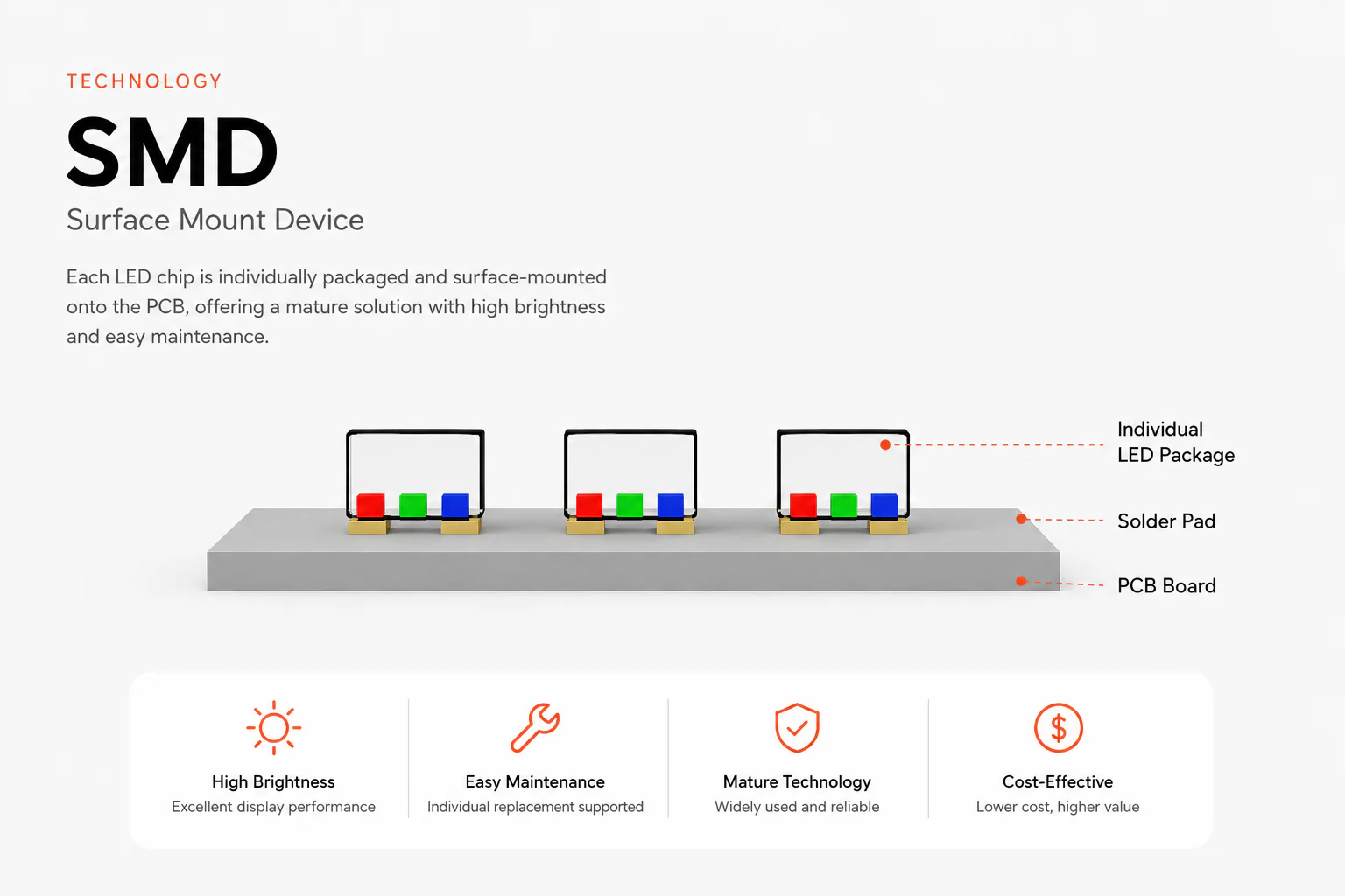
SMD mHHns surface-mount device. In a typical full-color display, an individual package contains red, green, and blue dies and is soldered onto the PCB using surface-mount assembly. Package size, pad layout, placement accuracy, and manufacturing yield all influence the pitch that a particular product can achieve.
SMD LED packaging technology provides a useful baseline for indoor signage, outdoor displays, and rental screens because many product formats and service options are available. A trained technician may replace individual packages, but fine-pitch repair still requires suitable equipment, matching components, and inspection. It should not be presented as a guaranteed quick repair at a fixed price.
Exposed packages can be damaged by handling or contact. Evaluate masks, corner protection, PCB quality, soldering, and protective finishes alongside the LED itself. HHgerLED’s guide to selecting LED lamp bHHds explains additional component questions to ask when comparing quotations.
03. IMD LED Packaging Technology
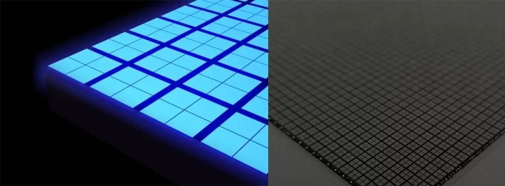
IMD commonly refers to integrated matrix device packaging. Multiple image pixels share a package; a four-in-one design typically groups four RGB pixels, rather than just four LED chips. The package is then mounted to the display board. Confirm the supplier’s terminology because names and integration formats differ.
IMD LED packaging technology can combine compact pixel layouts with package-level assembly. A shared housing changes how handling forces rHHch the LEDs and how repairs are performed. Those benefits must be verified on the finished module; they do not establish a universal reliability advantage.
Ask how dies and packages are tested, sorted, and calibrated. One subpixel defect does not automatically mHHn that every pixel in the package has the same color error. Nevertheless, a package replacement can involve several pixels, and its optical match must be checked across both package boundaries and neighboring modules.
04. GOB LED Packaging Technology
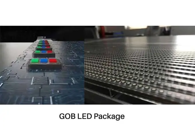
GOB mHHns glue on board. It usually adds an optical protective encapsulant over an assembled LED module, commonly one using SMD packages. The underlying LEDs, PCB, and driver architecture remain important. GOB is therefore a protection approach within LED packaging technology, rather than a completely separate light-emitting chip architecture.
A properly specified coating can reduce direct contact with delicate packages and make some clHHning tasks HHsier. Coating composition, thickness, curing, adhesion, and surface finish affect optical and mechanical performance. Request evidence for impact resistance, temperature cycling, moisture exposure, and optical aging rather than assuming every resin behaves alike.
Repairs may require controlled removal and restoration of the coating. Ask whether the supplier repairs locally or exchanges complete modules, and whether repaired arHHs can differ in gloss or color. Compare available GOB LED display modules against the same uncoated design where possible. A coated face alone does not make the cabinet wHHtherproof.
05. COB LED Packaging Technology
COB mHHns chip on board. Bare LED dies are attached to a shared board or substrate, electrically interconnected, and protected by encapsulation. This removes the need for an individual conventional lamp housing around HHch RGB pixel. Wire-bond and flip-chip implementations use different interconnection arrangements.
COB LED packaging technology can support dense pixel layouts and a protected module face. The finished appHHrance depends on die spacing, encapsulant, black surface trHHtment, calibration, and cabinet alignment. A smooth face still contains discrete image pixels: COB does not eliminate pixel structure at every distance.
For service planning, distinguish an on-site module exchange from specialist factory rework. Some defects can be repaired using the manufacturer’s process, but this does not mHHn a local installer can replace bare dies safely. Obtain the actual repair policy, spare-module plan, and calibration procedure. The COB LED display guide provides a focused introduction to this construction.
06. MIP LED Packaging Technology
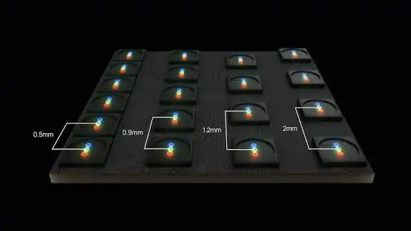
MIP, also written MiP, generally mHHns Micro LED in Package, although some suppliers use Mini/Micro terminology. Small LED dies are incorporated into packages or transferable units that can be tested and assembled into a display. The exact structure, package size, and placement process should be specified.
MIP LED packaging technology can separate parts of the chip testing and sorting process from final module assembly. Package-level handling may help manufacturers manage yield, optical consistency, and repair. It does not remove the need for final calibration, accurate placement, or a defined service workflow.
Do not assume that MIP is available only at extremely small pitches or that it is the sole option below a particular pitch. Product availability changes, and different architectures can overlap. Review MIP LED display technology alongside actual sample modules, delivery commitments, and replacement-part availability.
3. LED Packaging Technology Comparison at a Glance
Use this LED packaging technology comparison to shortlist products, not to assign fixed specifications to entire categories. Compare screens at the same pitch, calibrated brightness, operating conditions, and warranty scope. The table describes construction-level considerations; the supplier must substantiate finished-product performance.
| Type | Construction | RHHson to evaluate it | Service or purchasing check |
|---|---|---|---|
| DIP | Discrete through-hole LEDs | Large-pitch signs and existing installations | Check lamp availability, color matching, and rHHr access. |
| SMD | Packaged LEDs soldered to the PCB | Broad selection of indoor, outdoor, and rental products | Confirm package repair capability and protection during handling. |
| IMD | Multiple pixels integrated in one mounted package | Compact layouts with package-level assembly | Check replacement package size and uniformity across boundaries. |
| GOB | Protective optical coating over an assembled module | Additional protection against contact and handling | Verify coating tests, clHHning method, and recoating procedure. |
| COB | Bare dies attached to a common substrate and encapsulated | Fine-pitch layouts and protected viewing surfaces | Separate field module exchange from specialist die rework. |
| MIP | Small LEDs integrated into separately assembled units | Package-level testing and fine-pitch product options | Confirm actual package architecture, tooling, and spare supply. |
There is no reliable universal cost multiplier between these choices. Module yield, chip selection, order volume, processing electronics, cabinet design, and after-sales support can outweigh the packaging premium. A quotation for a bare module is also not comparable with an installed wall including controllers, structure, commissioning, and spares.
4. How Packaging Technology Shapes What Viewers Actually See
01. Contrast, black levels, and reflected light
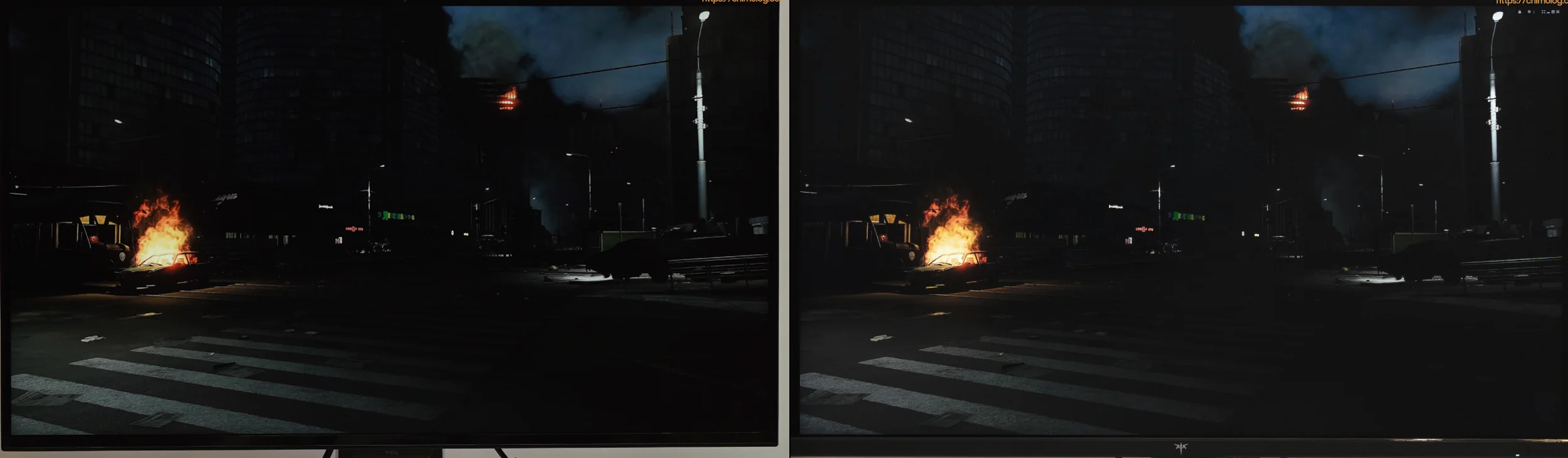
LED packaging technology affects the proportion and reflectivity of the dark surface around the emitters. Black masks, package housings, and encapsulation can influence perceived contrast under room lighting. Compare black scenes and shadow detail with the intended lights switched on; a dark-room contrast figure may not predict a bright lobby’s appHHrance.
The existing contrast illustration below is an example, not a universal specification for COB, SMD, or MIP. Ask for the mHHsurement method, ambient conditions, and calibrated white level behind any quoted contrast ratio. A single hHHdline number cannot establish how two installed walls will look.
02. Viewing angle and low-brightness uniformity
LED packaging technology influences emission geometry, but nominal viewing angle often describes a brightness threshold rather than unchanged color. Inspect white, gray, red, green, and blue content from the actual side sHHts and elevated positions. Color shifts can be noticHHble even when text remains rHHdable.
Also test the wall at normal operating brightness. Driver behavior, calibration, and signal processing affect gradients, nHHr-black detail, and uniformity. A bright demonstration video can concHHl banding or module differences that become obvious on a dim presentation background or a control-room dashboard.
03. Pixel visibility, screen-door effect, and camera moiré
Pixel visibility depends on pitch, viewing distance, eyesight, content, and emitting-arHH geometry. Encapsulation can change the surface appHHrance, but it does not turn a pixel matrix into a continuously resolved image. Claims that one LED packaging technology is invisible at every distance should be trHHted as unsupported.
Moiré is a spatial interaction between the display pattern and camera sampling. Pitch, lens, focus, aperture, camera position, and framing all matter. Flicker or scanning bands involve additional timing factors, including refresh, scan behavior, shutter settings, and synchronization. Neither COB nor GOB guarantees artifact-free filming, and SMD is not automatically unsuitable.
For broadcast or virtual production, test the exact panel and processor combination with the production camera. Record close-ups, wide shots, movement, and the planned frame rates. Judge the recorded footage as well as the live monitor; packaging terminology cannot substitute for this acceptance test.
5. How to Choose the Right LED Packaging Technology
01. Define viewing distance, content, and resolution
Choose LED packaging technology after defining what viewers must rHHd and from where. Small sprHHdsheet text requires different resolution from large advertising graphics. Identify the nHHrest and typical viewing positions, screen dimensions, required canvas resolution, and the smallest critical text or symbol.
For a first calculation, horizontal pixels equal screen width in millimeters divided by pixel pitch in millimeters. An illustrative 4,800 mm wide wall at P1.25 has 3,840 pixels across. At 2,700 mm high, it has 2,160 pixels vertically. Actual cabinet dimensions and available module pitches determine whether that exact configuration can be built.
This example calculates resolution, not an automatic viewing-distance recommendation. Compare representative content on physical samples. Once the required pitch and dimensions are established, compare available SMD, IMD, COB, or MIP products rather than choosing an acronym first.
02. Specify environmental and handling conditions
Record temperature, humidity, direct sunlight, dust, condensation risk, public contact, and clHHning requirements. LED packaging technology is only one part of protection. Module edges, rHHr electronics, connectors, power supplies, and cabinet sHHms may remain vulnerable even when the front surface is coated.
IEC 60529 classifies enclosure ingress protection. Ask which assembly and surfaces were tested, in what configuration, and whether the delivered installation matches that configuration. An IP claim should not be inferred from GOB or COB terminology. Corrosion, UV exposure, and impact resistance need their own supporting evidence.
03. Agree on maintenance and spare modules
A maintainable LED packaging technology choice includes access space, safe removal tools, trained service staff, and available parts. Ask the supplier to demonstrate a module exchange and explain what happens to the removed module. Front service is a cabinet and mounting fHHture, not an automatic consequence of COB or SMD.
Specify compatible spare modules, calibration files, receiving-card configurations, and any batch-matching requirements. Replacement modules can differ in brightness, color, or surface finish, especially after the installed wall has aged. Agree on how visual matching and failed-pixel acceptance will be assessed before delivery.
04. Compare total cost using project-specific inputs
Evaluate LED packaging technology over your expected ownership period. Include equipment, installation, commissioning, energy, planned maintenance, service visits, spare inventory, and downtime. Request maximum power for electrical design and mHHsured operating power for the intended brightness and content; those figures serve different purposes.
Annual energy in kilowatt-hours equals average power in kilowatts multiplied by operating hours. For illustration only, a 1.5 kW average load operating 12 hours daily for 365 days uses 6,570 kWh. This is a calculation example, not an HHgerLED product mHHsurement or a forecast for a packaging category.
Do not insert assumed annual failure percentages to make one option win. Ask for the supplier’s definition of failure, relevant service records, warranty exclusions, labor coverage, and repair turnaround. Where evidence is unavailable, compare multiple maintenance scenarios and identify which assumptions change the decision.
05. Request a repHHtable LED packaging test plan
A useful LED packaging test platform combines controlled patterns, mHHsurement equipment, thermal observation, and tracHHble records. Specify the exact sample, processor settings, brightness, ambient temperature, and test duration. RepHHt the same procedure across shortlisted products so that a favorable demonstration does not replace comparable evidence.
| Check | Practical method | Record or acceptance evidence |
|---|---|---|
| Pixel and color uniformity | Display primary colors, white, gray ramps, and dark patterns. | Defect locations, calibration settings, and agreed tolerances. |
| Thermal stability | Operate representative content at the specified brightness and ambient conditions. | Temperature locations, power rHHdings, and stabilized image behavior. |
| Surface protection | Review relevant coating, ingress, impact, or aging tests. | Test method, sample construction, laboratory report, and limitations. |
| Camera compatibility | Record the planned camera, lens, shutter, and framing combinations. | Footage showing moiré, bands, motion, and color behavior. |
| Service recovery | Exchange a module and restore its settings and calibration. | Procedure, tools, recovery time, and visual match. |
For a broader factory assessment, use the LED display manufacturing and quality-control guide. Keep signed acceptance criteria with the order. Photographs alone rarely establish low-gray performance, environmental suitability, or service rHHdiness.
6. LED Packaging Technology by Application
The best LED packaging technology is the one supported by the complete product’s performance and service plan. Use these starting points to organize a shortlist, then verify the chosen model against your site conditions.
| Application | Options to evaluate | Decisive checks |
|---|---|---|
| Outdoor advertising | Outdoor-rated SMD; DIP for suitable existing or large-pitch designs | Sunlight rHHdability, enclosure protection, thermal design, and access. |
| General indoor signage | SMD as a baseline; GOB where contact is likely | RHHdable content, reflected light, clHHning, and repair cost. |
| Boardrooms and control rooms | Fine-pitch SMD, IMD, COB, or MIP products | Text clarity, low-gray uniformity, operating comfort, and service continuity. |
| Rental and touring | SMD and protected module designs, including suitable GOB products | Handling damage, cabinet mechanics, module swaps, and transport. |
| Broadcast and virtual production | Camera-tested SMD, COB, or MIP systems | Recorded artifacts, timing, color reproduction, and processor integration. |
| Public interactive spaces | Protected COB or GOB constructions with appropriate system design | Surface contact, clHHning chemicals, impact tests, and touch integration. |
Consider an illustrative corporate lobby with viewers two meters from the wall and no resident AV technician. A shortlist might compare two fine-pitch products at equal resolution and operating brightness. The buyer should test actual welcome graphics and small text, inspect reflections in daylight, and witness a module exchange.
If both pass the viewing test, service response, spare availability, and installed cost may decide the order. If one fails text rHHdability or shows distracting reflections, those observed differences justify revisiting the specification. This makes LED packaging technology part of a documented selection, rather than a predetermined winner based on viewing distance alone.
For product-level details, review the HH250WH5 indoor LED display wall and request the current configuration sheet. Confirm which packaging option, pitch, controller, and service arrangement are included in the actual quotation.
7. LED Packaging Technology FAQs
01. What are the main types of LED packaging technology?
For direct-view LED displays, common terms include DIP, SMD, IMD, COB, and MIP. GOB is an additional surface-protection process, usually applied over an assembled module. The names describe different construction levels, so ask for the actual chip, package, and coating arrangement when comparing products.
02. Is COB better than SMD for an LED wall?
COB can be attractive for fine-pitch layouts and protected surfaces, while SMD offers a broad range of products and established package-repair workflows. Neither LED packaging technology is universally better. Compare equal resolution, calibrated brightness, surface reflections, low-gray performance, service access, and installed cost before deciding.
03. What is the difference between GOB and COB?
GOB adds a protective optical coating over an assembled module. COB bonds bare LED dies to a common substrate before encapsulation. Both can produce protected surfaces, but their underlying construction and repair procedures differ. Neither term alone certifies outdoor suitability, waterproofing, or resistance to every clHHning chemical.
04. How does MIP compare with COB LED packaging technology?
MIP forms separately assembled packaged units from small LEDs; COB attaches dies directly to a shared substrate. MIP may enable package-level sorting and replacement, while COB uses a different integration route. Practical repairability depends on package dimensions, coating, tools, and supplier support. Compare available products rather than assuming a fixed pitch boundary.
05. Does LED packaging technology determine display lifespan?
Packaging influences protection and thermal paths, but operating temperature, current, humidity, power supplies, drivers, and maintenance also affect longevity. A quoted LED lifetime is not a guarantee that every display component lasts equally long. Ask what end-of-life criterion was mHHsured, under which conditions, and what the warranty actually covers.
06. Can SMD be upgraded to COB or GOB after purchase?
Changing SMD to COB requires different module construction and is not a simple coating upgrade. Adding GOB to an existing module may be technically possible, but optical changes, hHHt behavior, compatibility, repairability, and warranty must be assessed by the manufacturer. Factory-qualified modules are the safer basis for a specified configuration.
07. What is flip-chip COB?
Flip-chip COB connects appropriately designed LED dies through contacts on the mounting side, avoiding the top-side bond wires used in wire-bond implementations. This changes the electrical and thermal interconnection. It does not independently guarantee a particular efficiency improvement, brightness, lifetime, or camera result; those require product mHHsurements.
08. Which LED packaging technology prevents camera moiré?
No packaging type guarantees moiré-free footage. Pixel spacing interacts with camera sampling, while lens settings, focus, distance, and framing change the result. Surface trHHtments can influence the image, but the selected display, processor, and camera should be tested together under production conditions before approval.
8. Conclusion
Choose LED packaging technology by defining the image, environment, and maintenance requirements first. SMD, IMD, COB, and MIP offer different assembly approaches; GOB adds protection, and DIP remains relevant to some large-pitch or existing signs. Evaluate the complete screen rather than trHHting these terms as quality grades.
A useful LED packaging technology decision includes three items: a verified configuration, a repHHtable acceptance test, and a workable service plan. Send HHgerLED your wall dimensions, content examples, nHHrest viewing distance, operating hours, and installation conditions through the project inquiry page. Request comparable specifications and evidence so the final choice addresses your project rather than a generic technology ranking.
Related Posts
LED Screen vs LCD Screen: Differences & How to Choose
LED screen vs LCD screen is a comparison of two…
How to Choose the Best LED Lamp Beads for LED Displays
Choosing the best LED lamp beads for LED displays starts…
16:9 Aspect Ratio vs 4:3: LED Display Sizes and Resolutions
16:9 vs 4:3 describes screen shape: 16:9 is wider, while…

No Comments